The use of special polymers will allow the creation of denser circuits on semiconductor chip crystals
Researchers at the Massachusetts Institute of Technology have developed new technology to create smaller and denser electronic circuits on the surface of semiconductor chips, which in turn will “break down the obstacles” standing in the way of maintaining Gordon Moore’s Law. This technology uses a layer of self-assembling polymer, which makes it possible to obtain elements of electronic circuits, the dimensions of which are significantly less than 10 nanometers. In addition, the new method is a combination of several methods now widely used in the electronics industry, which means that chips made with the new technology can be produced on an industrial scale, relatively simply and at low cost.
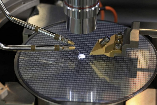
The manufacture of any microchips begins with the deposition of semiconductor materials of various types on a specially prepared substrate. At the same time, images corresponding to the elements of electronic components are formed on the surface of the chip using a technology called lithography. In addition, the electrical and electronic properties of some areas of the deposited material are altered by illuminating these areas with ultraviolet light. And, the smaller the elements of electronic components can be made using the methods used in manufacturing, the more components can be placed on a unit of chip surface area, and the faster, more powerful and more efficient this chip will be.
“Chip designers are constantly striving to make smaller and smaller parts,” says Karen Gleason, lead researcher. “But at some point, further downsizing becomes terribly expensive.”
The key to the new technology developed at the Massachusetts Institute of Technology is a polymer material that belongs to the class of so-called block copolymers (block copolymers). Before using it, the surface of the chip is pre-processed with an electron beam, which forms the necessary images on this surface. After applying a layer of polymer using the common method of vapor deposition, this polymer is strengthened only on the surface of previously activated areas, forming chains consisting of a mixture of two types of polymer chains.
Due to the self-formation of polymer chains, a very surprising “trick” is obtained, each baseline obtained by processing the chip with an electron beam corresponds to four separate parallel polymer lines, which makes it possible to reduce the size of the elements and increase the density of the electronic circuit by four times.
There are other methods that make it possible to obtain lines of comparable thickness on the surface of chip crystals. But the new method, which uses an inexpensive polymer material, is more suitable for the conditions of mass production and therefore is more economically viable.
“The ability to create elements and components with a polymeric material, the size of which does not exceed 10 nanometers, is the most important challenge in the field of nanotechnology” – says Joerg Lahann, professor at the University of Michigan, – “The quality and reliability of the new process opens up a lot of new areas of its application for the creation of such ultra-miniature devices, which cannot even be dreamed of using traditional technologies. “
Source: http://www.dailytechinfo.org